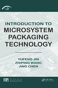
Introduction to Microsystem Packaging Technology
Об электронной книге
Introduction to Microsystem Packaging Technology details the latest advances in this vital area, which involves microelectronics, optoelectronics, RF and wireless, MEMS, and related packaging and assembling technologies. It is purposefully written so that each chapter is relatively independent and the book systematically presents the widest possible overview of packaging knowledge.
Elucidates the evolving world of packaging technologies for manufacturing
The authors begin by introducing the fundamentals, history, and technical challenges of microsystems. Addressing an array of design techniques for packaging and integration, they cover substrate and interconnection technologies, examples of device- and system-level packaging, and various MEMS packaging techniques. The book also discusses module assembly and optoelectronic packaging, reliability methodologies and analysis, and prospects for the evolution and future applications of microsystems packaging and associated environmental protection.
With its research examples and targeted reference questions and answers to reinforce understanding, this text is ideal for researchers, engineers, and students involved in microelectronics and MEMS. It is also useful to those who are not directly engaged in packaging but require a solid understanding of the field and its associated technologies.
Об авторе
Dr. Yufeng Jin received his Ph.D. degree in Electronical Engineering in March 1999 from Southeast University, Nanjing, China. Since then, he has been working as a postdoctoral fellow, an associate professor and a professor in Institute of Microelectronics, Peking University, China. Now he heads the National Key Laboratory of Science and Technology on Micro/Nano Fabrication at Peking University. From Nov. 2001 to Sept. 2004, he was a visiting research fellow in Singapore Institute of Manufacturing Technology for developing advanced MEMS packaging techniques. He worked with scientists and researchers in Applied Science and Technology Research Institute, HK as a consultant for 3D packaging development from Sept. to Nov. 2007. Current research interesting is mainly focused on advanced MEMS packaging, micro sensor, TSV-based 3D integration of microelectronics and its application systems.
Dr. Zhiping Wang received his D. Phil. degree in Engineering Science in March 1990 from Oxford University, UK. He had worked in Sheffield University, UK from March 1989 to April 1992. He then joined Singapore Institute of Manufacturing Technology, as research fellow, senior research fellow, and Group Manager for Joining Technology Group until August 2002, where he pioneered BGA, CSP, flip chip, and MEMS packaging technologies as well as interconnect reliability assessment methodology development. From September 2002 to June 2006, he worked in Industrial Technology Centre of Philips Mobile Display Systems as the Senior Manager of Module Technology, where he was responsible for display module technology development. He was the Chief Technology Officer of Advanpack Solutions Ptd Ltd in Singapore from Jun 2006 to Jan 2007. Since Feb 2007, he had been a Senior Scientist and the Programme Manager of Microfluidics Manufacturing Programme in Singapore Institute of Manufacturing Technology. His main interests are in the development of electronics packaging, MEMS packaging, and microfluidics technologies.
Dr. Jing Chen received his BS degree of Mechanical Engineering in 1997 from the Department of Precision Instrument and Mechanology, and Ph.D. degree of Electrical Engineering in 2002 from the Institute of Microelectronics, both in Tsinghua University, Beijing, China. After finishing his Ph.D., he worked as a postdoctoral research fellow for two years in the Solid-State Electronics Laboratory, the Department of Electrical Engineering and Computer Science, the University of Michigan. He has been working as an associate professor at the Institute of Microelectronics, Peking University since Sep. 2004. His major research focuses on micromachining techniques, RF MEMS and microsystem package. He has published more than 50 international journal papers and conference papers.


